
By simulating silicon vacancy energy, surface energy, and melting temperature, we showcase the ability of machine learning interatomic potentials (MLIPs) to simulate real properties relevant to semiconductor development. We show that fine-tuning in PHIN-atomic, an advanced active learning engine for MLIP-driven simulation, is necessary to accurately simulate the properties of real materials and is a significant improvement over pretrained models.
Silicon transistors inaugurated the information age by making digital computers exponentially less expensive. Over the past seven decades, their continuous advancement has propelled computing to a central position in our society through performance improvements predicted by Moore's Law. In the last 15 years, transistors have approached the physical limits of the planar process underpinning Moore’s law as nanometer gate sizes are composed of just a few atoms, significantly reducing the rate of innovation. New chip architectures like GPUs, TPUs, and ASICs seek to sidestep the slowing of Moore’s law by maximizing the performance of current chips, while new computing paradigms like neuromorphic and quantum computing signify a divergence from classical digital computing.
Moore’s law has however overcome previous physics barriers that questioned the supremacy of Moore’s law. High-k dielectrics and strained silicon are just two of these examples that propelled semiconductor manufacturing to follow Moore’s law for decades longer than predicted. The current physics barrier of nanometer gate sizes can similarly be solved with new material systems and manufacturing paradigms to continue the exponential decrease in computing cost.
Unfortunately, the cost of semiconductor materials development research has exponentially increased with time. To design the next manufacturing process, it is critical to find alternative methods of materials development, including in silico experimentation. A promising avenue is to use machine learning interatomic potentials (MLIPs) that reduce the cost of density functional theory (DFT) calculations by orders of magnitude. Here we show that when calculating industrially relevant material properties that inform the development of new semiconductors, pretrained MLIPs are not accurate enough, making it necessary to fine-tune machine learning models to the material system,eliminating hallucinations.
Using PHIN-OS and PHIN-atomic, we simulate a variety of critical properties related to semiconductor manufacturing and processing. We focus on the prediction of non-crystalline materials as case studies into the limits of pretrained models and to highlight the need for fine-tuning models with PHIN-atomic. In particular, we simulate the vacancy energy, the surface energy, and the melting temperature.
The vacancy energy is determined by a size scaling analysis, which varies the vacancy concentration. This allows computing the vacancy energy in the dilute limit, representing the energy of a single missing silicon atom. This method contrasts with the more common approach used with Density Functional Theory (DFT) calculations, which calculates the vacancy energy using the cohesive energy from a bulk calculation combined with a single vacancy calculation. The standard DFT method carries a higher risk of error in determining the appropriate size of the defected unit cell to correctly account for image interactions between defects. An example simulation workflow for the silicon vacancy energy is shown in Figure 1, where we can see the different branches used to simulate different vacancy concentrations and how they are all combined into a single vacancy analysis task. PHIN-OS natively allows for managing the data generated from dozens of these experiments to make more accurate methods attainable for all researchers.

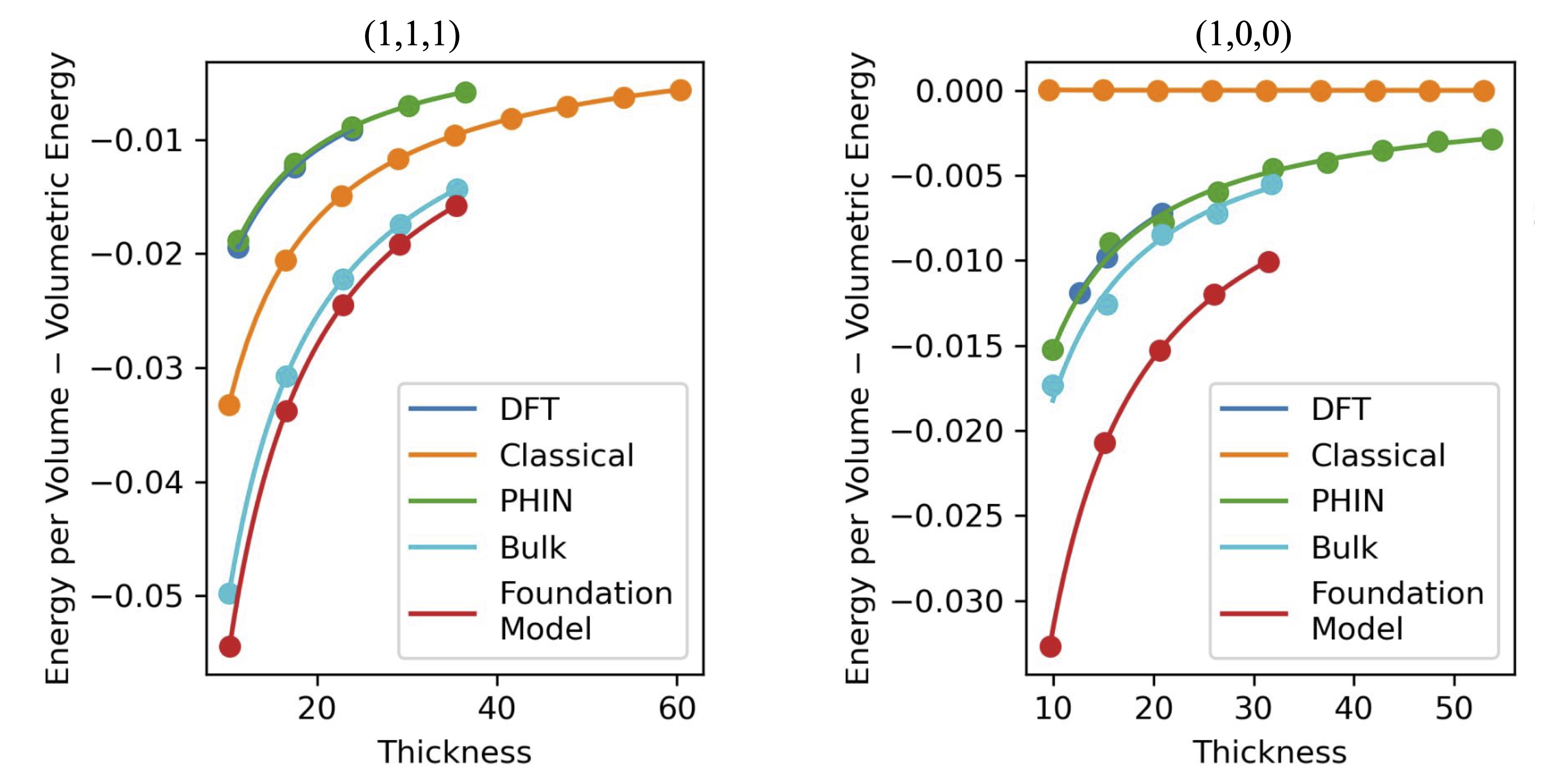
The surface energy is computed with a similar size scaling method, increasing the z dimension to sequentially increase the ratio of bulk to surface material. The total energy of the slab is composed of the bulk energy and the surface energy, which is extracted from a linear fit of the total slab energy as a function of the slab thickness. This reduces the risk of error due to neglecting the effect of the long-range interactions between the two surfaces in the simulation domain.
To predict the melting temperature, we use the SLUSHI method, which takes a supercell prepared from a crystalline solid and a melted structure to create a solid-liquid interface. The constructed supercell is used to run an NPT simulation where the solid-liquid interface moves to either solidify or melt the entire domain. The solid-liquid interface creates a heterogeneous nucleation site that has a much lower activation barrier for phase transformation enabling simulations of 100ps to be used for estimating the melting temperature. The simulation procedure requires running simulations at different temperatures to create a trace of solidification and melting configurations to reveal the temperature at which a phase transformation occurs.
For each material property we compare the two traditional techniques DFT and classical interatomic potentials (here Stillinger-Weber) against machine learning methods. We highlight our fine-tuned models against pretrained models to show the accuracy difference of next-generation machine learning methods and how they compare to the traditional techniques.
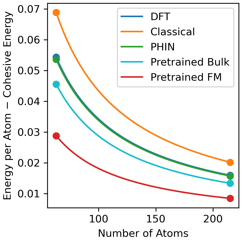
The results of the vacancy energy simulations are shown in Figure 2 revealing the excess cohesive energy of multiple structures with different vacancy concentrations. The best fit linear model for the vacancy energy versus the number of atoms shows the expected size scaling and extracts the predicted vacancy energies for each method. The vacancy energy calculated from PHIN-atomic almost perfectly agrees with DFT, whereas the pretrained foundation model underestimates the vacancy energy and the Classical model overpredicts the DFT vacancy energy. The pretrained Bulk model is in better agreement to DFT than the pretrained foundation model, which can be attributed to the amorphous atomic environments the model was trained on, which is not present in the pretrained foundation model dataset.
The near perfect agreement of PHIN to DFT highlights the power of PHIN’s software to reproduce DFT quantities, and the improvement of PHIN compared to its previous checkpoint (Pretrained Bulk) highlights the efficacy of PHIN’s active learning and uncertainty quantification. By showing the accuracy of PHIN’s models to zero Kelvin data, we establish confidence in the model’s ability to predict properties at the same accuracy as DFT. By establishing confidence in zero Kelvin data, we increase the confidence of using MLIPs in regions where it is too expensive to validate the with DFT data such as simulating the vacancy energy at room temperature. PHIN-atomic therefore provides trust in the values that are predicted by machine learning methods.
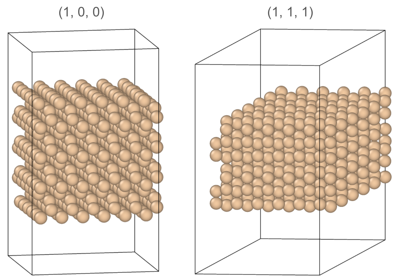
Silicon transistors are two dimensional devices constructed from wafers making it critical that MLIPs are able to simulate not just bulk materials with periodic boundaries but also at surface terminations. The crystalline nature of many materials means that there are a few preferential surface terminations that have significantly lower energies. The lowest energy surface terminations dictate the structure observed experimentally as well as how the material is faceted. For silicon, the diamond cubic crystal structure has two common surface terminations, defined by crystal lattice planes (1, 0, 0) and (1, 1, 1), the latter of which has lower energy and is therefore experimentally observed.
We simulate both surfaces with PHIN-atomic and compare it to the accuracy of classical and pretrained foundation models compared to DFT. The predictions from PHIN and DFT data are nearly indistinguishable in Figure 4, while all the other models significantly misestimate the surface energy. This quality of agreement is possible due to PHIN-atomic’s ability to actively learn any structures it is uncertain about. This means that the model is accurate not for the final structure, but of all the structures throughout the relaxations, which is necessary to arrive at the correct final structure.
Creating pristine silicon ingots with near zero defects uses a continuous solidification process by drawing solid silicon from a molten bath. The silicon crystallizes into a single crystal structure that is cut into wafers. Optimizing the solidification process of silicon is therefore essential for high yields in chips manufacturing. Historically, this melting process was optimized over decades using trial and error as the semiconductor industry matured. Painstaking decades of development resulted in near perfect single crystal ingots that are drawn from a melt.
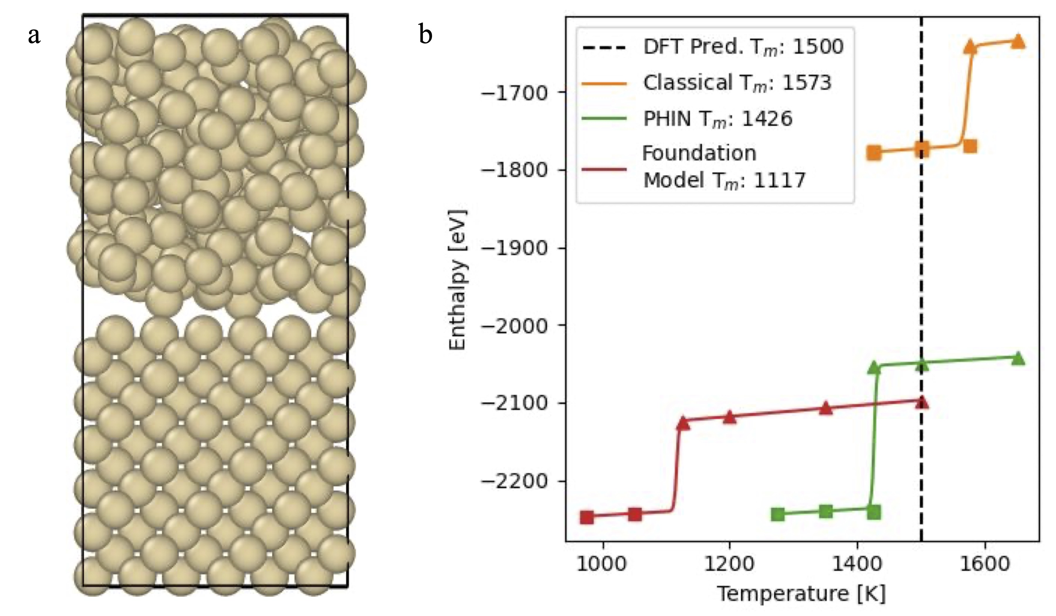
With MLIPs, we can simulate the solidification process with high accuracy. The SLUSHI method for determining the melting process resembles the drawing of silicon from a melt. As seen in Figure 5a below, the structures are initialized with a 50-50 blend of crystalline and amorphous silicon. The structures are simulated at different temperatures to give the enthalpies of each structure. The solid-liquid phase transition is clearly demarcated by an increase in the enthalpy of the structure. The resulting phase transition temperature shows the accuracy of PHIN’s model to DFT and a clear improvement on foundation models.
As machine learning interatomic potentials move from materials discovery to materials development, it is critical that machine learning interatomic potentials are able to accurately simulate the material properties necessary for developing materials. Using silicon as a case study for semiconductor materials, we investigate using PHIN’s MLIP’s within PHIN-atomic to simulate the vacancy energy, surface energy, and melting temperature. For these three properties, it is clear that pretrained models are not capable of simulating them accurately. PHIN-atomic’s automated fine-tuning algorithm is critical to simulating properties of real materials and allows for subsequent exploration of novel material systems (e.g., wide-bandgap semiconductors, 2D materials) and device architectures (3D semiconductors), providing deep physical insight that guides the experimental synthesis and optimization process.